
Category: Journal Papers
A Co-design Methodology for High-Performance Real-time Systems
Wael M. Badawy, Ashok Kumar and Magdy A. Bayoumi “A Co-design Methodology for High-Performance Real-time Systems” The Canadian Journal on Electrical and Computer Engineering, Vol. 26, July/October 2001, pp. 141-146.

System On Chip: Trends and Challenges
The increase in the number of transistors that can be integrated on a single chip allows the integration of more functions. On the other hand, time-to-market pressures require novel techniques for developing integrated circuits. System on chip is a methodology that allows the integration of several third-party cores with an embedded processor. This paper presents a tutorial for the system- on-chip methodology and presents the design tasks that are involved in developing a system on chip.
L’accroissement du nombre de transistors qu’il est possible d’inte ́grer sur une puce permet d’offrir plus de fonctionnalite ́s. D’autre part, les pressions de la mise en marche ́ rapide de celles-ci exige l’e ́laboration de techniques nouvelles de de ́veloppement de circuits inte ́gre ́s. Les syste`mes sur une puce repre ́sentent une me ́thodologie de de ́veloppement qui permet l’inte ́gration de com- posantes provenant de plusieurs de ́veloppeurs et de les combiner a` un processeur embarque ́. Cet article pre ́sente un tutoriel sur la me ́thodologie de conception de circuits sur une puce et pre ́sente les taˆches de design implique ́es dans le de ́veloppement de tels systemes.
Wael Badawy, “System On Chip: Trends and Challenges,” The Canadian Journal on Electrical and Computer Engineering, Vol. 26, July/October 2001, pp. 85-90.
MRI Data Compression Using a 3-D Discrete Wavelet transform
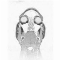
A low-power system that can be used to compress MRI data and for other medical applications is described. The system uses a low power 3-D DWT processor based on a centralized control unit architecture. The simulation results show the efficiency of the wavelet processor. The prototype processor consumes 0.5 W with total delay of 91.65 ns. The processor operates at a maximum frequency of 272 MHz. The prototype processor uses 16-bit adder, 16-bit Booth multiplier, and 1 kB cache with a maximum of 64-bit data bandwidth. Lower power has been achieved by using low-power building blocks and the minimal number of computational units with high throughput.
Published in:
Engineering in Medicine and Biology Magazine, IEEE (Volume:21 , Issue: 4 )
- Page(s):
- 95 – 103
- ISSN :
- 0739-5175
- INSPEC Accession Number:
- 7389345
- DOI:
- 10.1109/MEMB.2002.1032646
- Date of Publication :
- Jul/Aug 2002
- Date of Current Version :
- 07 November 2002
- Issue Date :
- Jul/Aug 2002
- Sponsored by :
- IEEE Engineering in Medicine and Biology Society
- Publisher:
- IEEE
Wael Badawy, Guoqing Zhang, Mike Talley, Michael Weeks and Magdy Bayoumi, “MRI Data Compression Using a 3-D Discrete Wavelet transform,” The IEEE Engineering in Medical and Biology Magazine, Vol. 21, Issue 4, July/August 2002, pp. 95-103.
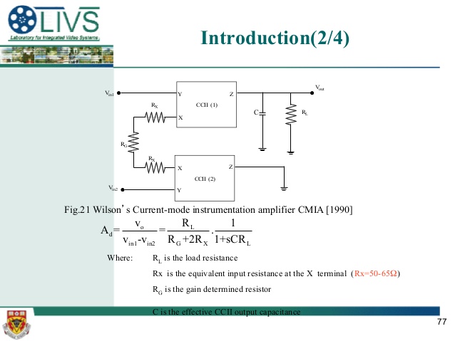
A Novel Current-Mode Instrumentation Amplifier Based on Operational Floating Current Conveyor,
This paper presents a novel current-mode instrumentation amplifier (CMIA) that utilizes an operational floating current conveyor (OFCC) as a basic building block. The OFCC, as a current-mode device, shows flexible properties with respect to other current- or voltage-mode circuits. The advantages of the proposed CMIA are threefold. First, it offers a higher differential gain and a bandwidth that is independent of gain, unlike a traditional voltage-mode instrumentation amplifier. Second, it maintains a high common-mode rejection ratio (CMRR) without requiring matched resistors, and finally, the proposed CMIA circuit offers a significant improvement in accuracy compared to other current-mode instrumentation amplifiers based on the current conveyor. The proposed CMIA has been analyzed, simulated, and experimentally tested. The experimental results verify that the proposed CMIA outperforms existing CMIAs in terms of the number of basic building blocks used, differential gain, and CMRR.
Published in:
Instrumentation and Measurement, IEEE Transactions on (Volume:54 , Issue: 5 )
- Page(s):
- 1941 – 1949
- ISSN :
- 0018-9456
- INSPEC Accession Number:
- 8601828
- DOI:
- 10.1109/TIM.2005.854254
- Date of Publication :
- Oct. 2005
- Date of Current Version :
- 03 October 2005
- Issue Date :
- Oct. 2005
- Sponsored by :
- IEEE Instrumentation and Measurement Society
- Publisher:
- IEEE
Yehya H. Ghallab, and Wael Badawy, Karan V.I.S. Kaler and Brent J. Maundy, “A Novel Current-Mode Instrumentation Amplifier Based on Operational Floating Current Conveyor,” IEEE Transaction on Instrumentation and Measurement, Volume 4, October 2005, pp. 1941 – 1949.

A VLSI Architecture for Video Object Motion Estimation using a Novel 2-D Hierarchical Mesh
This paper proposes a novel hierarchical mesh-based video object model and a motion estimation architecture that generates a content-based video object representation. The 2-D mesh-based video object is represented using two layers: an alpha plane and a texture. The alpha plane consists of two layers: (1) a mesh layer and (2) a binary layer that defines the object boundary. The texture defines the object’s colors. A new hierarchical adaptive structured mesh represents the mesh layer. The proposed mesh is a coarse-to-fine hierarchical 2-D mesh that is formed by recursive triangulation of the initial coarse mesh geometry. The proposed technique reduces the mesh code size and captures the mesh dynamics.
The proposed motion estimation architecture generates a progressive mesh code and the motion vectors of the mesh nodes. The performance analysis for the proposed video object representation and the proposed motion estimation architecture shows that they are suitable for very low bit rate online mobile applications and the motion estimation architecture can be used as a building block for MPEG-4 codec.
Wael Badawy “A VLSI Architecture for Video Object Motion Estimation using a Novel 2-D Hierarchical Mesh,” Journal of Systems Architecture, ISSN 1383 – 7621, invited

An Integrated Platform for Bio-Analysis and Drug Delivery
Seoud Amer, Wael Badawy, “An Integrated Platform for Bio-Analysis and Drug Delivery,” Current Pharmaceutical Biotechnology,, Volume 6, Issue 1, February 2005, pp. 57 – 64.

Analog IP Reuse in Nano Technologies, design and reuse
Analog IP Reuse in Nano Technologies
Hazem Said, Ain Shams University Cairo Egypt.
Mohamed Dessouky, Mentor Graphics Cairo Egypt.
Mohamed Tawfik, Mentor Graphics Cairo Egypt.
Quang Nguyen, ON Semiconductor Toulouse, France
Wael Badawy, University of Calgary, Calgary, Alberta
Hazem Abbas, Mentor Graphics, Cairo, Egypt
Hussein Shaheen, Ain Shams University, Cairo, Egypt
Abstract :
Presented in this paper is a tool that automatically migrates analog designs from one process to another while keeping circuit and layout topologies. A netlist migration engine recalculates the new device dimensions in the target technology followed by a layout migration engine that compacts the design according to the new process design rules. The overall framework preserves design intelligence embedded in the original IP such as symmetry, hierarchy, placement and routing. The circuit migration engine, being very fast, can retarget large analog blocks in only a few minutes while giving same or better performance of the original design. The migration of an integrated RC oscillator from 0.6u technology to 0.25u technology is presented to validate the overall methodology. This circuit has been fabricated and measured.
INTRODUCTION
Over the past few years there has been an interest toward cheap, low power portable electronics, which is driving the semiconductor industry to move toward more and more integration of functional blocks over a single IC in what is known as SoC design. The complexity of SoC designs nowadays is ever increasing and has resulted in more integration of mixed-signal blocks over a single IC. Driven also by the need to be more powerful, semiconductor manufacturers continue to innovate technologies towards smaller and smaller transistor feature sizes (for example from 0.25um to 0.18um to 0.13um). As a result, there is an increasing need in re-designing functioning mixed signal designs for new technology processes. Digital IP reuse is a well- established world thanks to the advance in the well-defined and automated digital flow available nowadays through different CAD companies. The analog domain on the other hand is still suffering from the lack of automation, which resulted in the analog IP portion being manually redesigned each time an SoC is migrated from a technology to another. This paper presents a complete framework, together with the associated tools, that retargets hard analog IP from one technology to another. The flow consists mainly of a circuit-sizing engine and a layout compaction engine. The benefit of this methodology is that it represents a complete solution to migrate hard IP between different processes in a fully automated way The rest of the paper is organized as follows: section 2 presents an overview of the state of the art for analog circuit migration techniques, section 3 presents the complete methodology for hard IP migration, section 4 presents the suggested circuit-sizing approach and a comparison versus other techniques, section 5 presents the suggested layout retargeting approach, section 6 presents examples and results. Finally section 7 presents a summary and draws conclusions of the work presented.
ANALOG DESIGN PROCESS MIGRATION
In order to migrate an analog hard-core IP from one technology to another all device dimensions in the target technology must be recalculated such as to get same circuit performance between source and target technologies. Several approaches have been investigated to resize the analog core of an SoC. One approach consists of developing specific block synthesis tools [1] [2]. These synthesis tools are developed specifically to cover a certain type of circuits like Opamps, PLLs, DACs or others. It should be noted that each type of these blocks could have several architectures. Each type of architecture has a different set of design equations and heuristics that describe the circuit. Hence, to develop such block synthesis tools, all design equations and heuristics be extracted and embedded within the tool. Block generator development takes a considerable effort and time. It must be justified by an extensive use of the generator. Design reuse based on an original working design has been investigated both through qualitative reasoning [3] and analog synthesis [4][5]. Another approach optimizes the equivalent small-signal model with respect to the original circuit [6]. The optimization engine visits candidate circuit designs and adjusts their parameters in an attempt to satisfy their user’s specified performance goals. A first group of optimization techniques use analytical models that describe the basic performance of the circuit using symbolic equations [7]. A second group of optimization techniques uses the full spice accuracy [8]. Using a full analog simulator capability has the advantage of accurate results but suffers from being very slow. On the other hand, using analytical equations has the impact of less accurate designs with faster results. The optimization techniques in general are closer to a circuit re-design than design reuse. All design knowledge and tradeoffs, implicitly coded by the first designer in the initial design, is completely lost. In addition, optimization-based techniques are only adapted to cell sizing due to their extensive use of computer resources. They are therefore less suitable for migrating a complete mixed-signal function (e.g. analog-to-digital converter, PLL, …).
COMPLETE MIGRATION FLOW
The complete migration flow is shown in Figure 1. The design that needs to be migrated should consist of a front-end view, in the form of a schematic/netlist (source circuit), and a back-end view, in the form of a layout (source layout) in a given process (source technology). The input to the resizing engine is the source netlist together with some technology information related to the source and target processes. The output of the resizing engine is a spice netlist with the new device dimensions that achieve the required circuit performance. Layout retargeting starts with a process layer mapping file in addition to the source layout. During a layer step, all layers in the source design are mapped to their corresponding layer in the target process. Addition or removal of layers is always possible between source and target processes. The following step involves the compaction of the layout while taking all design rules of the target process into consideration. New device sizes are considered as additional layout constraints. The output of the layout engine is a retargeted layout free of any design rule errors and updated with all device dimensions calculated from the circuit sizing engine.
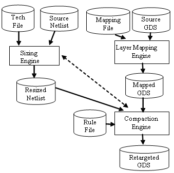
Figure 1. Migration Flow
CIRCUIT SIZING BASED ON DESIGN EXTRACTION
During circuit retargeting, the main focus is to keep the same circuit performance of a given circuit in a given fabrication process while trying to migrate it to a different fabrication target process. This is done hierarchically for the whole macro-function. Each block is handled separately in a specific order. Naturally, if the performance of each block is kept the same during design migration, the performance of the whole macro-function will also be the same.
The core of the methodology is based upon the definition of a relative transistor bias point as follows:
Itgt = KIsrc (1)
VGST = VGS – Vth (2)
VDST = VDS – VDSsat (3)
where K is a user-specified constant. Transistor electrical parameters and hence performance depends on the relative bias voltages rather than absolute voltages and currents.
The structure of the netlist migration engine is shown in Figure 2. The input to the engine consists of:
- Information about the source and target processes.
- A hierarchical netlist file in spice format.
- User defined constraints: K, fixing of some node voltages, minimum and maximum device dimensions.
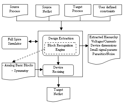
Figure 2. Structure of the netlist migration engine
As shown in Figure 2, the retargeting process itself is divided into two main actions: Design extraction and Device resizing. The design extraction engine is responsible of extracting all the knowledge embedded in the original design such as small signal parameters, large signal parameters, currents, node voltages, device dimensions, parasitics, and symmetry information. The design extraction engine is integrated with an interactive analog simulator that reads the structure of the netlist and extracts design hierarchy. A block recognition engine is embedded with the Design Extraction Engine and is capable of extracting different analog basic bulding blocks such as:
Current Mirror, Level Shifter, Voltage Reference, Current mirror Load, Differential Pair, Flip Flop, Current mirror block, Level Shifter Block, Current Source and Switch [9].
The device-resizing engine follows afterwards and is responsible of resizing the different devices in the circuit. The algorithm which is used to resize the transistors in the circuit is based on the assumption that preserving the parameters of each individual component (transistor, resistor, and capacitor) in each subcircuit would preserve the overall performance of each subcircuit, this would mean we would reach same performance of the overall circuit. In its first iteration, the engine scales all node voltages by the ratio of the old supply to the new supply voltage. The dimensions of the transistors are also scaled by the ratio of the old feature size to the new feature size.
In subsequent iterations the relative biasing points are kept the same between source and target technologies while the engine preserves the same small signals parameters of each device between source and target technologies by changing device dimensions in the target technology without exceeding the parasitics associated with each device.
The advantage of this method is that it doesn’t depend on any performance evaluation prior to reusing the circuit and hence there is no need to run multiple simulations to fit the device sizes to a certain performance criteria and hence the reuse cycle is very fast.
LAYOUT MIGRATION THROUGH PATH-FIXING EDGE BASED COMPACTION
As shown in Figure 1, layout migration is achieved using a compaction approach. Most existing compaction techniques use one-dimensional compaction, as in virtual grid [10][11], shear lines [12][13] and constraint graph [14] approaches. Compactors based on constraint graph approach generate better quality layouts [14]. Also, nearly all existing techniques use symbolic layouts, where layout elements represent devices or wires (symbols).
Solving a constraint graph to generate the compacted layout is done using the well-known longest path algorithm [14] [15]. However, some enhancements are still needed to minimize wire length [16].
In this engine, rather than using a symbolic approach, the constraint graph handles edges of layout polygons directly. A path-fixing technique based on graph-theory is used for minimization of polygon areas. This graph-based technique produces a compacted layout without the need of time consuming simplex matrix operations.
Figure 3 shows a sample layout together with the corresponding constraint graph. The constraint graph is a directed graph in which nodes represent edges of layout polygons, while arcs represent a distance constraint between two edges represented by the two end nodes of the arc. For example, an arc from node x1 to node x9 with a length of 10 represents the following distance constraint: x9 – x1 ? 10. A distance can either be a width constraint or a separation constraint. A width constraint determines the minimum width of a certain polygon. It exists between two edges of the same polygon inside the polygon, e.g. [x1, x9] and [x3, x4]. A separation constraint is a constraint between two edges of the same polygon, but outside the polygon, or the edges of two different polygons that determine the minimum separation between these two edges. For example, arcs between [x4, x5] and [x8, x9] are separation constraints. Two artificial edges are added at both extremities to bound edge movement as shown in figure 3(b).
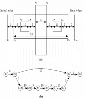
Figure 3. (a) sample layout and (b) the corresponding constraint graph
A path is a series connection of arcs in the same direction with no node touched more than once. As can be seen from Figure 3(b), two paths exist between node x1 and node x9: [x1, x9] with a length of 10 and [x1, x3, x4, x5, x6, x7, x8, x9] with a length of (5+10+5+10+5+10+5)= 50. A compaction path is defined as the longest path between two edges xi, xj, which have a minimum width constraint between them. For example nodes x1, x9 have minimum width constraint between them represented by the arc [x1, x9]. The compaction path between x1, x9 is therefore [x1, x3, x4, x5, x6, x7, x8, x9].
The algorithm aims to find the location of each edge in the layout to minimize the total areas of layout polygons while respecting design rules. It associates location bounds to each edge, in addition to a fixed flag that indicates that this edge can not move anymore.
The algorithm produces a compacted layout with no need to wire length minimization or post processing [16]. It depends mainly on graph-based operations that are more efficient than linear programming matrix operations usually used in wire length minimization. Dealing with edges other than symbols enables the compaction engine to handle any complex device and any complex routing.
Initial layout contains valuable knowledge, and in most cases already verified by fabrication. The migration by compaction keeps the same knowledge (i.e. floor-planning, placement, routing) in the target layout. Layer mapping used in the migration engine allows complex devices to be migrated even to completely different layers.
EXAMPLE AND RESULTS
This section shows an industrial test case that has been identified to validate and test the migration tool. This is an integrated RC Oscillator which has been migrated from a 0.6u to a 0.25u process of two different foundries to increase porting challenges. The overall CPU run time for both resizing and layout migration of the design took less than one hour on an Ultra Sparc machine where 80% of the time is consumed by the layout migration engine.
Integrated RC Oscillator.

Figure 4. Oscillator Frequency vs supply
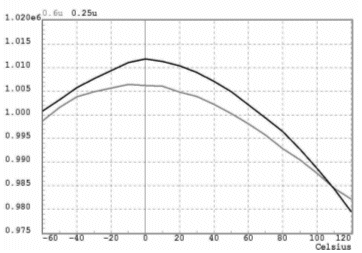
Figure 5. Oscillator Frequency vs temperature
This is an integrated astable oscillator that produces a 1 MHz output frequency. It has an output frequency with very high stability versus temperature sweep from –55 to 125°C. The output frequency is very stable as well with supply variations from 2.5 to 5.5V. The oscillator contains several blocks such as a bandgap reference, some biasing cells, a digital decoder used for trimming, an amplifier and a couple of comparators. The number of devices inside this circuit is around 500. The migration of the design from 0.6u to 0.25u took 1 week including corner simulation and post layout verification. Figure 4 and Figure 5 show simulation results of the source and migrated oscillator versus temperature and supply voltage sweep respectively. The maximum variation in frequency between the source and target designs is less than 1% when sweeping over the temperature and less than 4% for supply change. This is an acceptable variation especially that the oscillator has a trimming circuitry that enables fine adjustments over the frequency of the oscillator. Figure 6 shows the source layout with an area of around 93600u2 while Figure 7 shows the retargeted layout with an area of around 86400u2 saving around 8% which is less than the previous examples due to the large area occupied by passive devices.
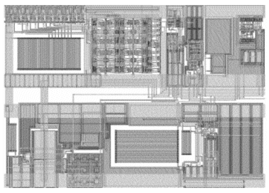
Figure 6. Oscillator layout in 0.6u technology
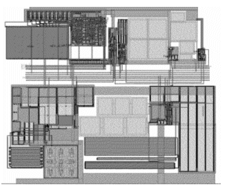
Figure 7. Oscillator layout in 0.25u technology
CONCLUSION
This paper described an innovative method for the reuse of analog circuits; this method includes both a circuit sizing engine for circuit migration and a layout-retargeting engine. The circuit-sizing engine is based on design extraction and device performance mapping. The layout engine is based on a modified edge-based compaction algorithm. Both netlist and layout engines are efficient with small cells as well as macro-functions and have proven to be very fast. The validation of the tool has been demonstrated by retargeting and fabricating a real design through an industrial partnership.
REFERENCES
[1] R.R. Neff, P.R Gray, and A. Sangiovanni-Vincentelli, “ A Module Generator for High-Speed CMOS Current Output Digital/Analog Converters”, in IEEE J. of Solid State Circuits, Vol. 31, pp. 448-451, Mar. 1996.F. Medeiro, B. Pérez-Verdú, A. Rodríguez-Vázquez, and J. L. Huertas, “A Vertically Integrated Tool for Automated Design of ?? Modulators”, in IEEE J. of Solid State Circuits, Vol. 30, pp. 762-772, Jul. 1995. [2] K. Francken, and G. Gielen, “Methodology for Analog Technology Porting Including Performance Tuning”, in Proc. IEEE Int. Symp. On Circuits and Systems, Vol. 1, pp. 415-418, May 1999. [3] R. Phelps, M. Krasnicki, R. Rutenbar, L. R. Carley, and J. Hel-lums, “A case study of synthesis for industrial-scale analog IP: Re-design of the equalizer/filter frontend for an ADSL CODEC,” in Proc. ACM/IEEE Design Automation Conf., pp. 1–6, 2000. [4] E. Hennig, R. Sommer and L. Charlack, “An Automated Approach for Sizing Complex Analog Circuits in a Simulation-Based Flow”, in Proc. ACM/IEEE Design Automation and Test in Europe, Designer Forum, pp. 230-234, Mar. 2002. [5] S. Funaba, A. Kitagawa, T. Tsukada, and G. Yokomizo, “A Fast and Accurate Method of Redesigning Analog Subcircuits for Technology Scaling”, Analog Integrated Circuits and Signal Processing, Kluwer Academic Publishers, Vol. 25, 2000, P. 299-307 [6] C.Toumazou and C.Makris, “Analog IC design automation: Part I—Automated circuit generation: New concepts and methods, ” IEEE Trans. Computer-Aided Design, vol.14, pp. 218–238, Feb.1995. [7] Xu Jingnan; Serras, J.; Oliveira, M.; Belo, R.; Bugalho, M.; Vital, J.; Horta, N.; Franca J. “IC design automation from circuit level optimization to retargetable layout,” ICECS 2001. The 8th IEEE International Conference on Circuits and Systems, Volume: 1, Sept. 2001 pp. 95 – 98 vol.1. [8] H. Graeb, S. Zizala, J. Eckmueller, and K. Antreich, “The Sizing Rules Method for Analog Integrated Circuit Design”, in Proc. Int. Conf. on Computer-Aided Design, pp. 343 – 349, 2001. [9] Weste, N. “Virtual Grid Symbolic Layout”, in Proc. the 18th Design Automation Conference, June 1981, pp. 225-233. [10] Bayer, D-G.; and Weste, N. “Virtual Grid Compaction Using the Most Recent Layers Algorithm”, in Proc. ICCAD, 1983, pp. 92-93. [11] A.E. Dunlop, “SLIM – The Translation of Symbolic Layouts into Mask Data”, in Proc. of the 17th Design Automation Conference, IEEE (1980), 595 – 602 [12] A.E. Dunlop, “SLIP: Symbolic Layout of Integrated Circuits with Compaction”, Computer Aided Design, November 1978. [13] Y. E. Cho, “A subjective review of compaction”, in Proc. 22nd Design Automation Conf., June 1985, pp. 396–404. [14] D. G. Boyer, “Symbolic layout compaction review,” in Proc. 25th Design Automation Conf., June 1988, pp. 383–389. [15] D. Marple. “A hierarchy preserving hierarchical compactor”, in Proc. 27th Design Automation Conference, 375-381, 1990.Sherif Hammouda, Hazem Said, Mohamed Dessouky, Mohamed Tawfik, Quang Nguyen, Wael Badawy, Hazem Abbas, Hussein Shaheen, “Analog IP Reuse in Nano Technologies, design and reuse,” April 6, 2006.
An Efficient Architecture for a Lifted 2D Biorthogonal DWT
This paper presents a new algorithm for a 2D non-separable lifted bi-orthogonal wavelet transform. The algorithm is derived by factoring complementary pairs of wavelet transform 2D filters. The results are efficient architectures for real time signal processing, which do not require transpose memory for the 2D processing of data. The proposed architecture exploits in place implementation, inherit from the algorithm, and can take advantage of both vertical and horizontal parallelism in the direct implementation. The processing in our architecture is scheduled by carefully pipelining the lifted steps, which allows for up to four times faster processing than the direct implementation. The proposed architecture operates at high speed, consumes low power and has reduced computational complexity as compared to previously published filter and lifted based bi-orthogonal wavelet architectures.
Mehboob Alam , Wael Badawy, Vassil Dimitrov and Graham Jullien, “An Efficient Architecture for a Lifted 2D Biorthogonal DWT,” The Journal of VLSI Signal Processing , Volume 40, Issue 3, July 2005, pp. 335 – 342
A Proposed Hardware Reference Model for Spatial Transformation and Quantization in H.264,
This paper presents three Very Large Scale Integration prototypes to exploit spatial redundancy in the H.264 standard. The proposed architectures are: (1) forward 4 × 4 integer approximation of DCT transform and quantization, which is applied to all blocks of a frame, (2) the 4 × 4 Hadamard transform and quantization that is applied to the DC coefficients of the luma component when the macroblock is encoded in 16 × 16 intra prediction mode, and (3) the 2 × 2 Hadamard transform and quantization that is applied to the DC coefficients of the chroma component as a second level in the transformation hierarchy. The developed algorithms are adopted by the H.264 standard. A performance analysis shows that the architectures satisfy the real-time constraints required by different digital video applications.
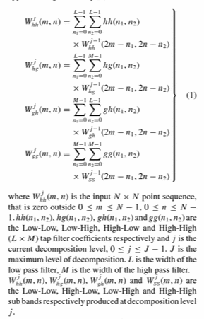
I. Amer, W. Badawy, G. Jullien, “A Proposed Hardware Reference Model for Spatial Transformation and Quantization in H.264,” Elsevier Journal of Visual Communication and Image Representation, Volume 17, Issue 2, April 2006, Pages 533-552.

An Affine Based Algorithm and SIMD Architecture for Video Compression with Low Bit-rate Applications
This paper presents a new affine-based algorithm and SIMD architecture for video compression with low bit rate applications. The proposed algorithm is used for mesh-based motion estimation and it is named mesh-based square-matching algorithm (MB-SMA). The MB-SMA is a simplified version of the hexagonal matching algorithm [1]. In this algorithm, right-angled triangular mesh is used to benefit from a multiplication free algorithm presented in [2] for computing the affine parameters. The proposed algorithm has lower computational cost than the hexagonal matching algorithm while it produces almost the same peak signal-to-noise ratio (PSNR) values. The MB-SMA outperforms the commonly used motion estimation algorithms in terms of computational cost, efficiency and video quality (i.e., PSNR). The MB-SMA is implemented using an SIMD architecture in which a large number of processing elements has been embedded with SRAM blocks to utilize the large internal memory bandwidth. The proposed architecture needs 26.9 ms to process one CIF video frame. Therefore, it can process 37 CIF frames/s. The proposed architecture has been prototyped using Taiwan Semiconductor Manufacturing Company (TSMC) 0.18-μm CMOS technology and the embedded SRAMs have been generated using Virage Logic memory compiler.
Published in:
Circuits and Systems for Video Technology, IEEE Transactions on (Volume:16 , Issue: 4 )
- Page(s):
- 457 – 471
- ISSN :
- 1051-8215
- INSPEC Accession Number:
- 8891917
- DOI:
- 10.1109/TCSVT.2006.872780
- Date of Publication :
- April 2006
- Date of Current Version :
- 01 May 2006
- Issue Date :
- April 2006
- Sponsored by :
- IEEE Circuits and Systems Society
- Publisher:
- IEEE
Back to a complete list of Peer-Reviewed Journal Papers
Mohammed Sayed , Wael Badawy, “An Affine Based Algorithm and SIMD Architecture for Video Compression with Low Bit-rate Applications“, IEEE Transactions on Circuits and Systems for Video Technology, Vol. 16, Issue 4, pp. 457-471, April 2006. Abstract